1 郑州大学物理学院,河南 郑州 450001
2 河南仕佳光子科技股份有限公司,河南 鹤壁 458030
面向多路射频模拟信号的高线性传输需求,基于强度调制-直接探测的原理,提出了基于波分复用技术的模拟射频光传输方案;利用高线性度模拟直调半导体激光器、波分复用器、模拟光电探测器,设计了基于微波光子技术的波分复用射频光传输链路,该链路具有低串扰、低失真、链路增益可调等性能。利用该链路进行了直调激光器、驱动控制电路、射频光发射模块和光接收模块的样机研制。对所研制出的样机进行了实验测试。测试结果表明:通道增益可在-30~10 dB调谐,通道内基波与二次谐波抑制比高于50 dB,相邻及非相邻通道间射频串扰均低于60 dB,相位一致性在±5°以内。针对不同的信号输入功率,在线调整链路增益,改善链路的信噪比或非线性失真效应。设计和研制的样机可用于低频段射频信号的光纤传输。
光纤通信 射频光传输 直调半导体激光器 模拟光链路 激光与光电子学进展
2023, 60(5): 0506005
1 科技部高技术中心材料处, 北京 100044
2 中国科学院半导体研究所 集成光电子学国家重点联合实验室, 北京 100083
3 中国科学院大学 材料科学与光电技术学院, 北京 100049
4 中国科学院大学 材料与光电研究中心, 北京 100049
二氧化硅平面光波导(PLC)器件以其低损耗、高工艺容差, 以及与CMOS工艺兼容和与单模光纤模场匹配良好等优点, 在光通信、光互连和集成光学中得到了广泛的应用。文章综述了二氧化硅平面光波导器件及其应用的进展, 重点针对分束器、阵列波导光栅、可调光衰减器及其集成器件的最新研究进行了介绍, 对未来发展趋势进行了展望。
有源光子集成波导器件 无源光子集成波导器件 集成光学 光通信系统 active photonic integrated waveguide devices passive photonic integrated waveguide devices integrated optics optical communication system
Author Affiliations
Abstract
1 State Key Laboratory on Integrated Optoelectronics, Institute of Semiconductors, Chinese Academy of Sciences, Beijing 100083, China
2 Center of Materials Science and Optoelectronics Engineering, University of Chinese Academy of Sciences, Beijing 100049, China
3 Division of Quantum Materials and Devices, Beijing Academy of Quantum Information Sciences, Beijing 100193, China
4 Laboratory of Quantum Information, CAS, University of Science and Technology of China, Hefei 230026, China
Quantum key distribution (QKD) provides a solution for communication of unconditional security. However, the quantum channel disturbance in the field severely increases the quantum bit-error rate, degrading the performance of a QKD system. Here we present a setup comprising silica planar light wave circuits (PLCs), which is robust against the channel polarization disturbance. Our PLCs are based on the asymmetric Mach–Zehnder interferometer (AMZI), integrated with a tunable power splitter and thermo-optic phase modulators. The polarization characteristics of the AMZI PLC are investigated by a novel pulse self-interfering method to determine the operation temperature of implementing polarization insensitivity. Over a 20 km fiber channel with 30 Hz polarization scrambling, our time-bin phase-encoding QKD setup is characterized with an interference fringe visibility of 98.72%. The extinction ratio for the phase states is kept between 18 and 21 dB for 6 h without active phase correction.
Photonics Research
2021, 9(2): 02000222
1 河南仕佳光子科技股份有限公司, 河南 鹤壁 458030
2 郑州大学物理学院, 河南 郑州 450001
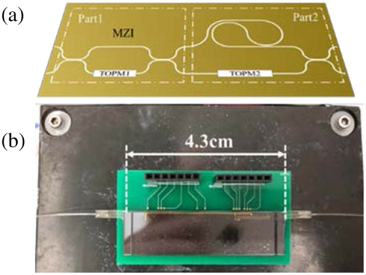
设计制备了一种低功耗的马赫-曾德尔干涉仪(MZI)型聚合物热光开关器件,为降低开关的功耗,将器件加热区的调制臂波导设计成悬浮波导,从而抑制波导芯区处热量向硅衬底的扩散。模拟结果显示,相比于传统波导结构的热光开关,悬浮波导结构可以明显减少热扩散。利用半导体工艺成功制备了具有悬浮波导结构的热光开关器件,在1550 nm工作波长下,热光开关的功耗为9.3 mW,消光比为21 dB,开关的上升和下降时间分别为392 μs和697 μs。
集成光学 集成光学器件 热光开关 聚合物波导 功耗 消光比
1 郑州大学物理学院, 河南 郑州 450001
2 河南仕佳光子科技股份有限公司, 河南 鹤壁 458030
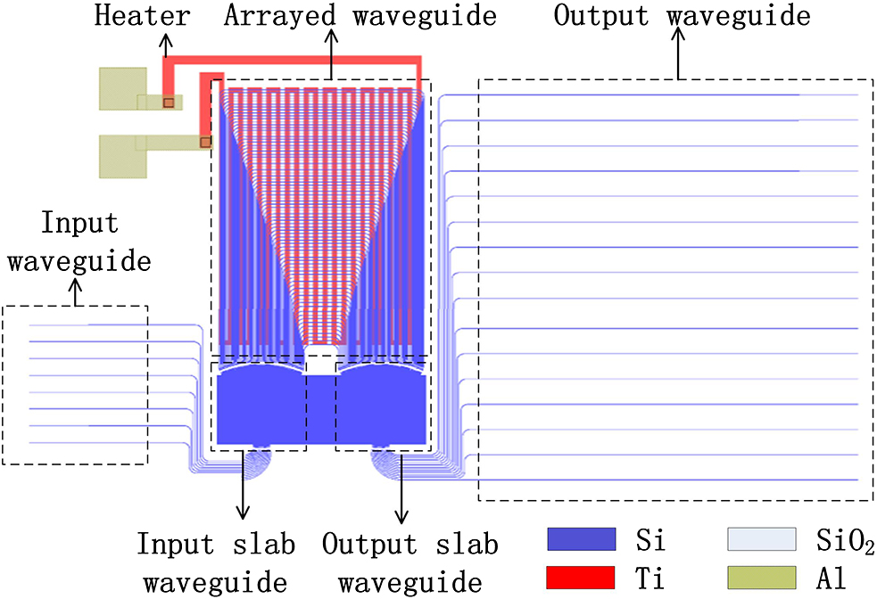
对硅基二氧化硅阵列波导光栅解复用器(AWG DEMUX)的偏振相关损耗(PDL)进行了优化。理论分析了引起AWG偏振相关性的物理因素以及消除偏振相关性的工艺方法和条件。利用化学气相沉积、光刻和刻蚀等半导体工艺制备了AWG DEMUX芯片,并结合理论分析对包层材料中的硼(B)、磷(P)含量进行了优化调整,成功地将芯片的PDL降低至0.12 dB,使PDL参数满足芯片的商用化需求。
光通信 阵列波导光栅 解复用器 偏振相关损耗
1 北京信息科技大学 光纤传感与系统北京实验室,北京 100016
2 中国科学院半导体研究所 集成光电子学国家重点实验室,北京 100083
3 中国科学院大学 材料与光电研究中心,北京 100049
刻蚀衍射光栅作为波分复用/解复用器件,有望在光通信系统中得到广泛应用。在基于顶层硅厚度为220 nm的绝缘体上硅材料上设计并制作了一种新型刻蚀衍射光栅,该刻蚀衍射光栅引入六角晶格空气孔型光子晶体作为其反射镜。模拟结果显示,相较于传统的阶梯光栅反射镜的刻蚀衍射光栅,光子晶体反射镜的刻蚀衍射光栅在理论上可有效降低器件的制作工艺难度以及插入损耗,同时可以实现器件偏振的保持。随后仅利用一步电子束光刻工艺及一步电感耦合等离子体刻蚀工艺制作了该光子晶体反射镜的刻蚀衍射光栅。测试结果表明:该光子晶体反射镜的刻蚀衍射光栅片上损耗为9.51~11.86 dB,串扰为5.87~8.72 dB,后续可通过优化工艺条件和优化输出波导布局,进一步提高器件的性能。
刻蚀衍射光栅 光子晶体 硅基光子学 波分复用/解复用 etching diffraction grating photonic crystal silicon photonics wavelength division multiplexing/de-multiplexing 红外与激光工程
2019, 48(9): 0916005
1 北京信息科技大学 光纤传感与系统北京实验室, 北京 100016
2 中国科学院半导体研究所 集成光电子学国家重点实验室, 北京 100083
3 中国科学院大学 材料与光电研究中心, 北京 100049
波分复用/解复用器与可调光衰减器的是光通信系统中的重要元器件。为了得到制备工艺简单、响应速度快的二者的单片集成芯片, 并且考虑到其与其他不同光器件的集成可能性, 在绝缘体上硅材料制作了16通道、信道间隔200 GHz的阵列波导光栅复用/解复用器与电吸收型可调光衰减器的单片集成。该器件的片上损耗小于7 dB, 串扰小于-22 dB。电吸收型VOA在20 dB的衰减量下的功耗为572 mW(106 mA, 5.4 V)。此外, 该器件可以实现光功率的快速衰减, 在0~5 V的外加方波电压下, VOA上升及下降时间分别为50.5 ns和48 ns。
阵列波导光栅 可调光衰减器 硅基光子学 绝缘体上硅 arrayed waveguide grating variable optical attenuator silicon photonics silicon on insulator 红外与激光工程
2019, 48(8): 0818004
1 中国科学院半导体研究所集成光电子学国家重点联合实验室, 北京 100083
2 中国科学院大学材料科学与光电技术学院, 北京 100049
论述了光学相控阵的原理,回顾了光学相控阵的发展历程,特别是近年来硅光子相控阵的研究进展。利用与互补金属氧化物半导体(CMOS)工艺线相兼容的绝缘体上硅(SOI)技术实现了大规模的集成,目前国外报道的最大的硅光子相控阵集成了4096个阵元。在硅光子上实现的二维光束扫描角度可以达到46°×36°,光束宽度只有0.85°×0.18°,天线的损耗小于3 dB,且旁瓣抑制大于10 dB。此外,采用微机电系统(MEMS)器件实现的光学相控阵的光束扫描速度超过0.5 MHz。阐述了各种方式实现光学相控阵的优缺点,并对未来发展前景进行了展望。最后,介绍了光学相控阵在激光雷达、成像、**上的应用。
光学器件 光波导 光学相控阵 扫描角度 绝缘体上硅 激光与光电子学进展
2018, 55(2): 020006
Author Affiliations
Abstract
1 State Key Laboratory on Integrated Optoelectronics, Institute of Semiconductors, Chinese Academy of Science, Beijing 100083, China
2 College of Materials Science and Opto-Electronic Technology, University of Chinese Academy of Sciences, Beijing 100083, China
In this Letter, a 16 channel 200 GHz wavelength tunable arrayed waveguide grating (AWG) is designed and fabricated based on the silicon on insulator platform. Considering that the performance of the AWG, such as central wavelength and crosstalk, is sensitive to the dimension variation of waveguides, the error analysis of the AWG with width fluctuations is worked out using the transfer function method. A heater is designed to realize the wavelength tunability of the AWG based on the thermo-optic effect of silicon. The measured results show that the insertion loss of the AWG is about 6 dB, and the crosstalk is 7.5 dB. The wavelength tunability of 1.1 nm is achieved at 276 mW power consumption, and more wavelength shifts will gain at larger power consumption.
060.1810 Buffers, couplers, routers,switches, and multiplexers 060.4230 Multiplexing 230.7390 Waveguides, planar Chinese Optics Letters
2018, 16(1): 010601

Author Affiliations
Abstract
1 State Key Laboratory of Integrated Optoelectronics, Institute of Semiconductors, Chinese Academy of Sciences, Beijing 100083, China
2 College of Materials Science and Opto-Electronic Technology, University of Chinese Academy of Sciences, Beijing 100049, China
Both the 4×20 GHz coarse wavelength division multiplexing and LAN-WDM receiver optical sub-assemblies (ROSAs) were developed. The ROSA package was hybrid integrated with a planar lightwave circuit arrayed waveguide grating (AWG) with 2% refractive index difference and a four-channel top-illuminated positive-intrinsic-negative photodetector (PD) array. The output waveguides of the AWG were designed in a multimode structure to provide flat-top optical spectra, and their end facet was angle-polished to form a total internal reflection interface to realize vertical coupling with a PD array. The maximum responsivity of ROSA was about 0.4 A/W, and its 3 dB bandwidth of frequency response was up to 20 GHz for each transmission lane. The hybrid integrated ROSA would be a cost-effective and easy-assembling solution for 100 GbE data center interconnections.
060.4230 Multiplexing 230.7370 Waveguides Chinese Optics Letters
2018, 16(6): 060603


